


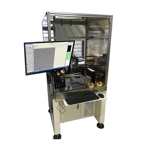
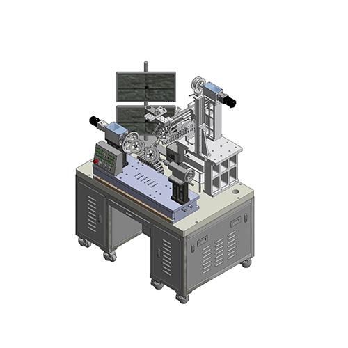
The shape and distribution of dislocation defects in semiconductor wafer preparation have a significant impact on the performance of electronic components. Due to differences in doping materials and preparation processes, the distribution of dislocations also varies. This device is used to inspect the morphology and distribution of wafer dislocations, providing data support for wafer material research and improving preparation processes. Suitable for 2-inch, 3-inch, 4-inch, and 6-inch gallium arsenide substrates.
Tags :
View More


 Consultation Hotline:86-0592-3799658、86-137 9991 1773(Switchboard)